One of the problems I have when designing PCBs, or working in CAD with a view to 3D printing it is easy to lose sight of how big things on the screen are in real life.
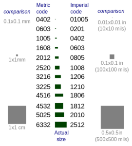
A lot of the time when you move away from working with through-hole components towards SMD your components move away from a nice convenient 2.54 mm pitch and onto obscure sizing such as the image to the right:
This is just a list of two terminal passives such as Resistors, Capacitors and Inductors (Tantalum and Aluminium capacitors have different sizing as well). As you can see from the image the packages are a little small and hard to envisage.
Thinkl33t managed to get a Digi-Key ruler, I have been after getting one like this, but I have not been able to find one I like (NVIDIA also has a nice one):
Online there are several different designs showcasing people’s work
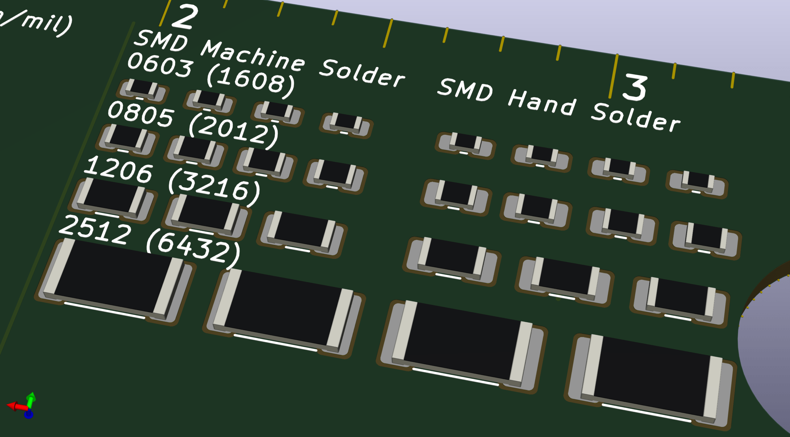
Kicad is shipped with a range of passive footprints, at the sizes of 0603/1608 (0.6 mm × 0.3 mm), 0805/2012 (2.0 mm × 1.25 mm), 1206/3216 (3.2 mm × 1.6 mm), and 2512/6432 (6.3 mm × 3.2 mm) there are two versions, the normal ones, and ones that are ‘suitable’ for hand soldering. And this is before we move on to smaller or more complicated components.
I am working on making my PCBs that I can hand out and use as a reference for designing PCBs. on the other side, I plan on putting a small circuit for people to have a go at soldering.
If KiCAD doesn’t have the parts or footprints you need, then you can make your own going from the data sheet to 3D model, Component, and schematic.


