
When you have been using KiCad for a while to make PCBs, one of the things you will come to find is a pain is that by default the KiCad grid origin is set up in the top left of the Paper Space, which makes it a bit of a pain to use the position X and Y coordinates system. I assumed that someone must have written an online tutorial on how to move the origin. However, despite looking for instructions for moving the PCB Grid Origin, I ended up raising a support ticket.
The Origin (0,0) in the properties dialogue is outside the frame in paper space, The ability to move the origin would allow for easier setup of PCB edge.cuts, as well as placement of components on the PCB. as the Start Point, and the grid would have the same origin.
Support Ticker #15628
Then I was informed in the ticket the functionality already exists in KiCad, and the ticket was closed with the following information:
You could already set the origin to different positions:
- global Preferences –> pcb editor –> Origins & axes –> Display origin –> use drill file origin / use grid origin
Maik Freitag in support ticket #15628
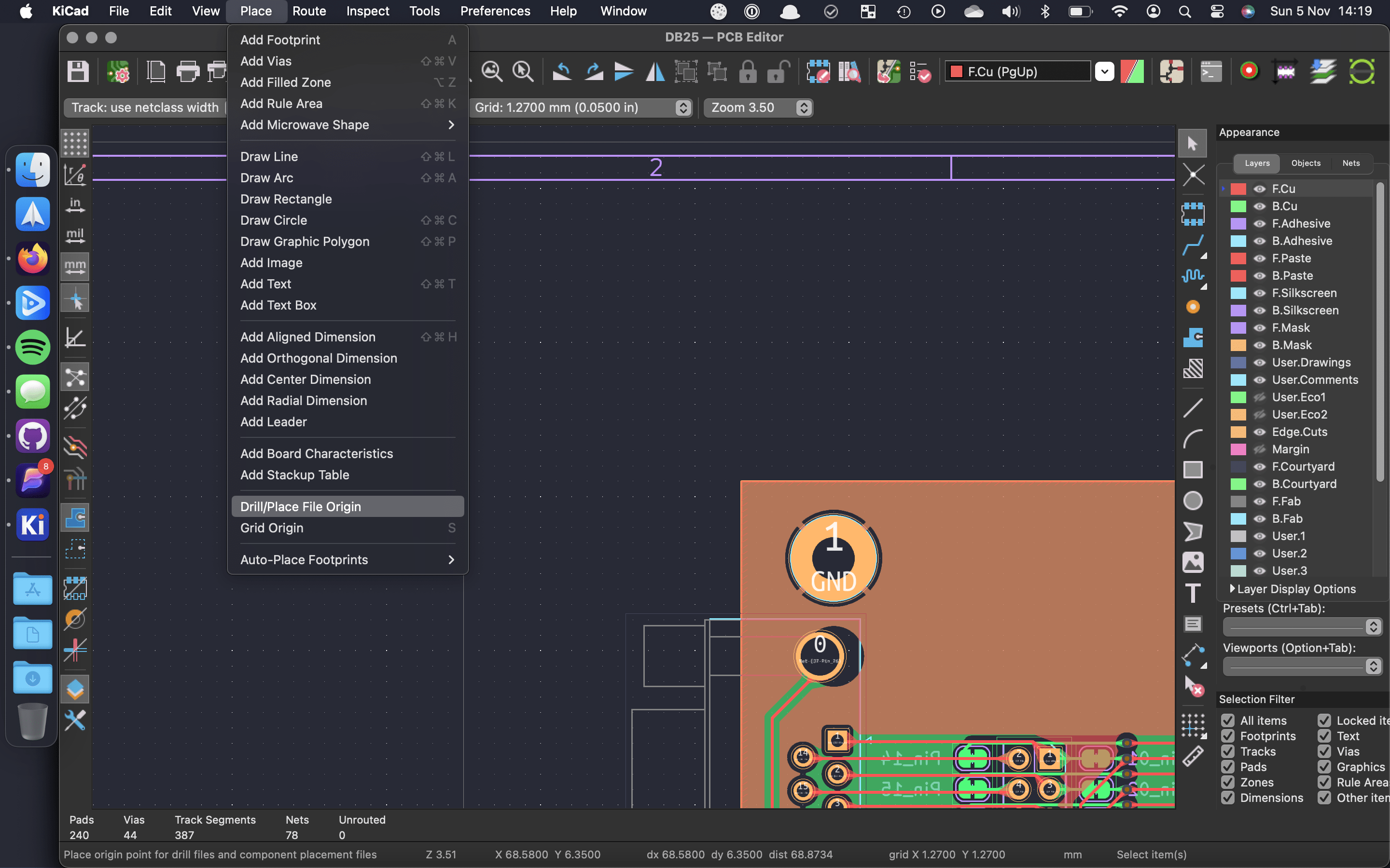
- subsequently set the drill/grid origin point to any desired location (main menu –> Place –> set drill origin/set grid origin)
The Default location of the Origin
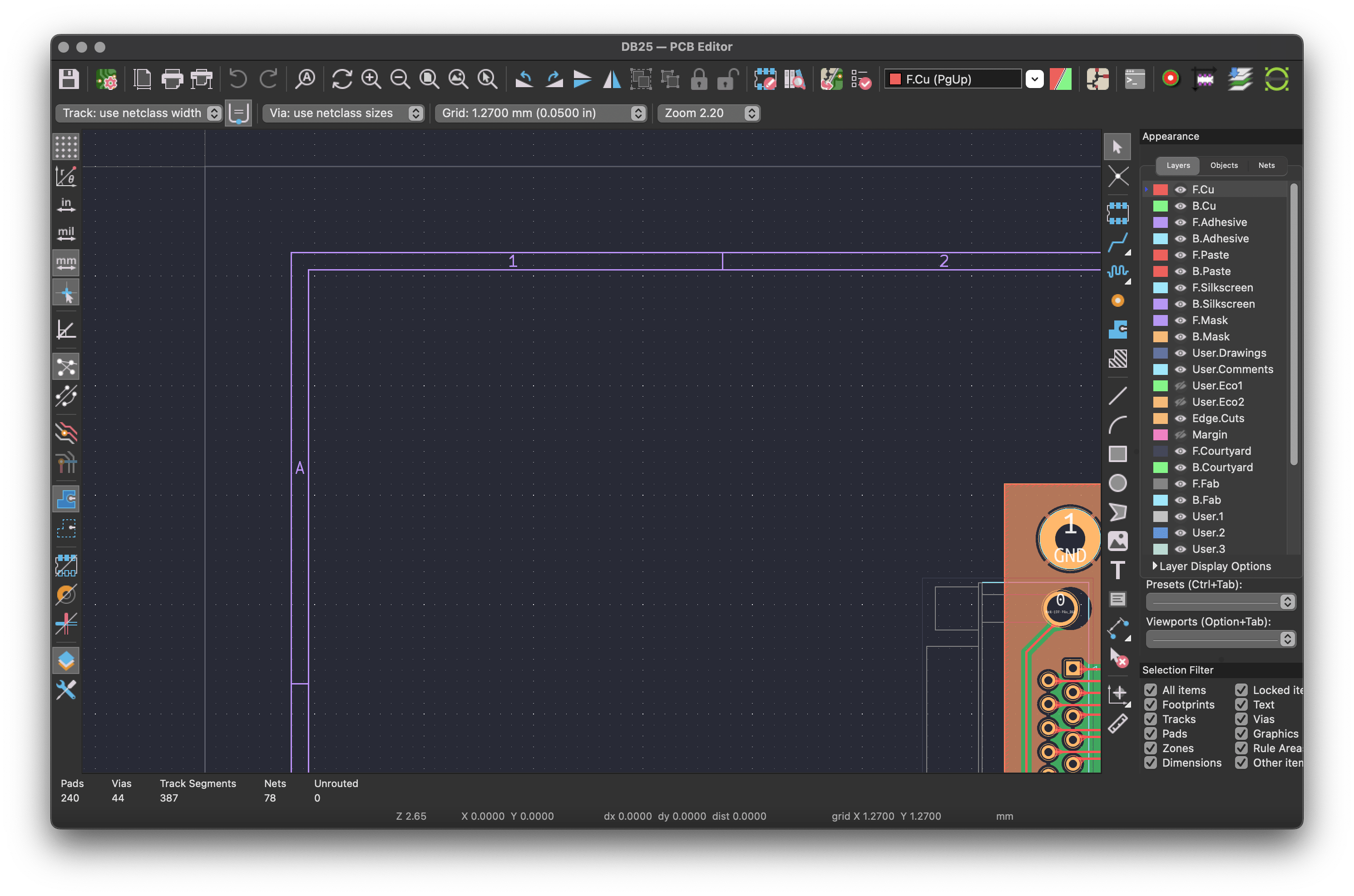
As you can see from the above image the cursor is on the origin, X and Y in the status bar read 0,0.
Moving the Origin
the instructions from above are “global Preferences –> pcb editor –> Origins & axes –> Display origin –> use drill file origin / use grid origin”
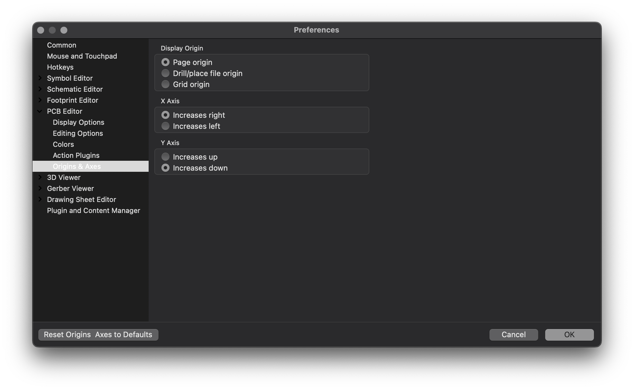
There are three choices for “Display Origin”, Page origin, Drill/place file origin, and Grid origin.
Display Origin
This is the default origin and is the top left corner of the Paper Space. the origin that I am trying to move away from,
Drill/Place file origin
This is the first of the two origins that we can customise the location of, the Drill/Place file is normally used by PCB fabrication houses when fabricating your PCBs. For PCBs (I normally get my PCBs made up by PCB Way).


Grid Origin
I place the grid origin in the same location as I place the Drill/place file origin, and in the preferences choose the Grid Origin as my display origin
 and Drill/place file origin at the same location in KiCad PCB editor (KiCad 7).")


20 thoughts on “KiCad PCB Grid Origin”
Another shortcut we use all the time is the “Space bar” key to reset local origin. Very useful for doing spot check measurments.
I will have to give that one a go next time I am trying to measure something 🙂
This and your article on auto routing are very helpful. I’m saving these links so I hope you maintain this site for sometime.
Thank you 🙂 there will be more posts some time soon.
Oh wow, didn’t know about it !
Origin point outside of the PCB area and reversed Y-axis has always irritated me.
Good to know it can be changed in the latest KiCAD revisions.
Is there no easy way to move the origin in kicad?
In 6 its easy, like a mouse click and a key press or something like that. Not sure about 7
Press and hold here for pop up menu to select grid origin placement
One the top Menu “Place” > grid origin (or hotkey S ) and / or Place > drill/place file original. And then place them in the position you want. I usually place them both in bottom left corner of the ocb outline (and change preferences > PCB editor > orogina and axis > X axis increase right and Y axis increase Up, but that’s my habit, set it as you wish if you prefer to have it differently).
I also found this tutorial, maybe you’ve seen it.
11 minutes of listening to a video for something that should take less than five minutes…
Agree
Are you using V6? This is what I saw in a blog post if you are.
“Long-press with the left mouse button, or click and drag with the left button.” I don’t know if that works just passing it along.
I am using KiCad v7.0
Easy solution – use DipTrace, or if you can afford it, Altium.
While DipTrace Starter is $75, which is only 2 layers and 300 pins, the minimum package that supports 4 layer PCBs is DipTrace Standard at $395, and that supports 1000 pins, 4 signal layers… it doesn’t take long to need more than 1000 pins.
Altium doesn’t support multiple OSs
However, in the spirit of giving Diptrace a go, I am downloading the mac version to have a go.
Correct, but it is so intuitive that I willingly paid the price after comparing to the price of pro tools like Altium. Much more affordable and almost as useful. I use Altium when I am working for a company that can afford it, and it isn’t such a big deal to use Windows for it. Sorry if you prefer Macs for engineering uses, you are in the minority.
Ugh, I kind of need to design a PCB and I dread it. It’s a whole level of learning I’m just not ready for yet.
Start small, pick up a copy of one of Forrest M. Mims III’s books, and build a few circuits on a solderless breadboard, then once you are happy you know what it does, try laying it out in KiCad
I think for now I will stick with dev kits and cannibalizing other things, but at some point I will need specialized boards if for no other reason but that it can be designed to fit the spaces they need to fit.