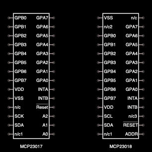
In my previous post, I talked about some of the advantages of the MCP23018, and how it was easier to address…
Well, it turns out that I made the standard mistake of not reading the datasheet…
It’s not as though the MCP23018 obscures the lack of current source deep in the datasheet, the sub-heading of the datasheet is literally “16-Bit I/O Expander with Open-Drain Outputs”, yet however after reading the datasheet several times, even some of the specifications:
MCP23018 Features:
- 16-bit remote bidirectional I/O port
- I/O pins default to input
- Open-drain outputs:
- 25 mA sink capable (per pin)
- 400 mA total
- High-speed I2C interface:
- 100 kHz
- 400 kHz
- 3.4 MHz
- Single hardware address pin:
- Voltage input to allow up to eight devices on the bus
- Configurable interrupt output pins:
- Configurable as active-high, active-low or open-drain
- Configurable interrupt source:
- Interrupt-on-change from configured defaults or pin change
- Polarity inversion register to configure the polarity of the input port data
- External reset input
- Low standby current:
- 1 μA (-40°C≤TA≤+85°C)
- 6 μA (+85°C≤TA≤+125°C)
- Operating voltage:
- 1.8 V to 5.5 V
If we compare that to the MCP23017s datasheet:
- 16-Bit Remote Bidirectional I/O Port:
- I/O pins default to input
- High-Speed I2C Interface:
- 100kHz
- 400kHz
- 1.7MHz
- Three Hardware Address Pins to Allow Upto Eight Devices On the Bus
- Configurable Interrupt Output Pins:
- Configurable as active-high, active-low or open-drain
- INTA and INTB Can Be Configured to Operate Independently or Together
- Configurable Interrupt Source:
- Interrupt-on-change from configured register defaults or pin changes
- Polarity Inversion Register to Configure the Polarity of the Input Port Data
- External Reset Input
- Low Standby Current: 1 μA (max.)
- OperatingVoltage:
- 1.8 V to 5.5 V@ -40°C to +85°C
- 2.7 V to 5.5V @ -40°C to +85°C
- 4.5 V to 5.5 V @ -40°C to +125°C
Further, into the MCP2307s datasheet, we get to §1.0 “Electrical Characteristics, Absolute Maximum Ratings”, which states that the maximum output current sunk by any output pin is 25 mA, maximum output current sourced by any output pin 25 mA, with the maximum current into the VDD (+5 V) pin being 125 mA, so less than 8 mA per output at full drive.
The MCP23018 datasheet has similar information under §2 “Electrical Characteristics, Absolute Maximum Ratings”, which states that the maximum output current sunk by any output pin is 25 mA, maximum output current sourced by any output pin 25 mA, with the maximum current into the VDD (+5 V) pin being 125 mA.
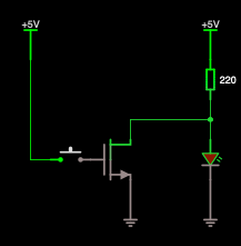
However, in the case of the MCP23018, it looks like this limit is for when the device is being used as an input, or for turning the output off, the Open Drain outputs, in the image to the right, you can see when they are in their off state, the LED is on, (the N-FET is internal to the MCP23018), and when the FET is in the on state, the LED will be off.
- When the internal FET is ON, the output would be LOW(0).
- When the internal FET is OFF, the output would be HIGH(1).
I could use an additional FET to not the output of the internal FET, however, this would also require a number of additional supporting components (including resistors).
Going back to the MCP23017, this IC seems to have a push-pull output stage, this is made up of two FETS (One P-FET, and one N-FET).
I will talk about the MCP23017s output stage in more length in a subsequent post.


2 thoughts on “MCP23017 vs MCP23018 and why I was wrong…”
Good lesson. ALWAYS consult the device datasheet. The devil is in the details.
Thanks so much! This is very helpful